Introduction
Bathymetric LIDAR (Light Detection and Ranging) is a powerful remote sensing technology used for precise mapping of underwater topography. By emitting short laser pulses toward a water body and measuring the time delay of reflected signals from both the water surface and the seafloor, LIDAR systems enable high-resolution three-dimensional reconstruction of submerged terrain. This capability is essential for various applications, including coastal zone management, hydrographic surveying, environmental monitoring, and flood risk assessment.
Traditional bathymetric LIDAR systems predominantly rely on photomultiplier tubes (PMTs)1,2 or avalanche photodiodes (APDs)3 for photon detection. While effective, these detectors exhibit limitations in terms of size, operating voltage, mechanical sensitivity, and photon detection efficiency under turbid or low-illumination aquatic conditions. Moreover, increasing environmental demands for more compact, energy-efficient, and UAV-compatible LIDAR systems necessitate the adoption of alternative photodetector technologies.
Silicon Photomultipliers (SiPMs) have emerged as a compelling alternative due to their ability to operate in Geiger-mode, enabling single-photon sensitivity, high gain, and excellent timing resolution. Unlike traditional PMTs, SiPMs are solid-state devices,4 offering advantages such as low bias voltage (20–70 V), immunity to magnetic fields, ruggedness, and potential for miniaturization and mass production. The high photon detection efficiency (PDE), particularly in the green and blue-green spectral bands optimal for water penetration (e.g., 515–550 nm), further strengthens their relevance for bathymetric LIDAR.5
Bathymetric LIDAR system
Bathymetric LIDAR (Light Detection and Ranging) is a laser-based remote sensing technology used to map underwater topography by measuring the time delay between the emission of laser pulses and the detection of their reflections from both the water surface and the seafloor. Mounted on aerial platforms such as drones, aircraft, or satellites, the system is designed to capture high-resolution, three-dimensional spatial data over shallow and coastal water bodies. The core principle of operation relies on the time-of-flight (ToF) method,6 where the system calculates the distance traveled by light by measuring the interval between pulse emission and reception (Fig. 1).
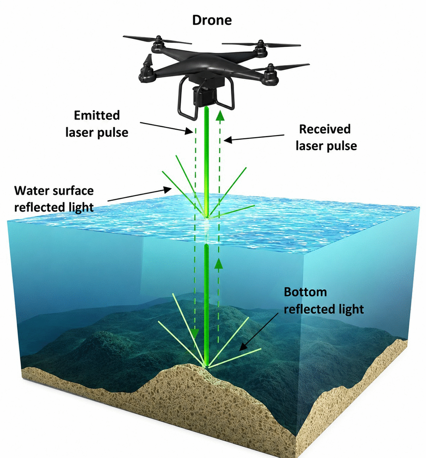
Figure 1. Schematic diagram of the bathymetric LiDAR system illustrating the time-of-flight (ToF) measurement principle.
Figure 1. Working principle of bathymetric LIDAR.
A typical bathymetric LIDAR system consists of a pulsed laser transmitter, an optical scanning unit (such as an oscillating mirror), a photodetector, and precise timing electronics, integrated with a positioning system that combines GNSS (Global Navigation Satellite System) and inertial measurement units (IMU). Among these components, the photodetector—most commonly implemented using silicon photomultiplier (SiPM) technology—plays a central role in determining the overall system performance. In particular, the photon detection efficiency (PDE) of the SiPM is one of the key parameters governing the signal-to-noise ratio, depth detection capability, and ultimately the spatial and depth resolution of the reconstructed bathymetric image. During operation, the system emits a laser pulse—most commonly in the green region of the visible spectrum (around 530 nm)—which is particularly suitable for water penetration due to its low absorption in clear water. Upon hitting the water surface, part of the pulse is reflected back and recorded as the first return, while the remaining energy penetrates the water column, reflects off the seafloor, and returns as the second signal. The difference in travel time between these two returns allows for the accurate determination of water depth using the relation
7 where c is the speed of light in vacuum and n is the refractive index of water, approximately 1.33. The improvements in photodetector sensitivity—particularly through the use of high-PDE SiPMs—directly translate into enhanced timing precision, improved depth retrieval, and higher-quality bathymetric images.
Photodetector concepts and comparison
In the context of bathymetric LIDAR systems, the choice of photodetector architecture plays a pivotal role in defining the system’s sensitivity, linearity, and reliability under low-photon conditions such as turbid or deep aquatic environments. Conventional SiPMs predominantly utilize surface pixel architectures, in which the photosensitive avalanche region is located directly beneath the top layer. While widely adopted due to their manufacturability and compactness, surface-pixel SiPMs are inherently limited by reduced fill factor and photon losses due to reflective metal routing and passivation layers on the surface,8–10 (figure 2 a-Model MPPC S12572-010P). The conventional architecture is based on a surface-pixel layout composed of microcells integrated onto a common silicon substrate 1. The substrate is typically fabricated using the Czochralski or float-zone method, ensuring high crystalline purity and suitable electrical conductivity for avalanche multiplication. Each microcell, or pixel 2, has a lateral size of 10 μm, which directly influences the detector’s fill factor and spatial resolution. Central to the functionality of each pixel is the quenching resistor 3, a thin-film component with resistance of 100 kΩ. This resistor ensures that the avalanche process, once triggered by a single photon event, is rapidly quenched to allow for pixel recovery and repeated detection. A common contact bus 4 distributes the bias voltage uniformly across all pixels. Each pixel connects to the bus via its dedicated quenching resistor, supporting independent operation and minimizing dead time. To prevent unwanted edge breakdown and premature triggering near the periphery of the device, a guard ring 5 is employed. This ring suppresses high electric field concentrations at the detector’s boundaries, thereby enhancing breakdown voltage uniformity and improving overall stability. The contact area 6 comprises metalized regions that provide electrical access to the external circuitry. It is carefully designed to avoid significant obstruction of incident light. The photosensitive area 7 represents the active region of the SiPM where incoming photons are absorbed and generate electron-hole pairs; optimizing this region for minimal reflection and high transparency is essential for maximizing PDE. Finally, the avalanche area 8, located within each pixel, contains the p-n junction designed to operate in Geiger mode. When a photon-induced carrier enters this region, it initiates an avalanche multiplication event, producing a detectable signal pulse.
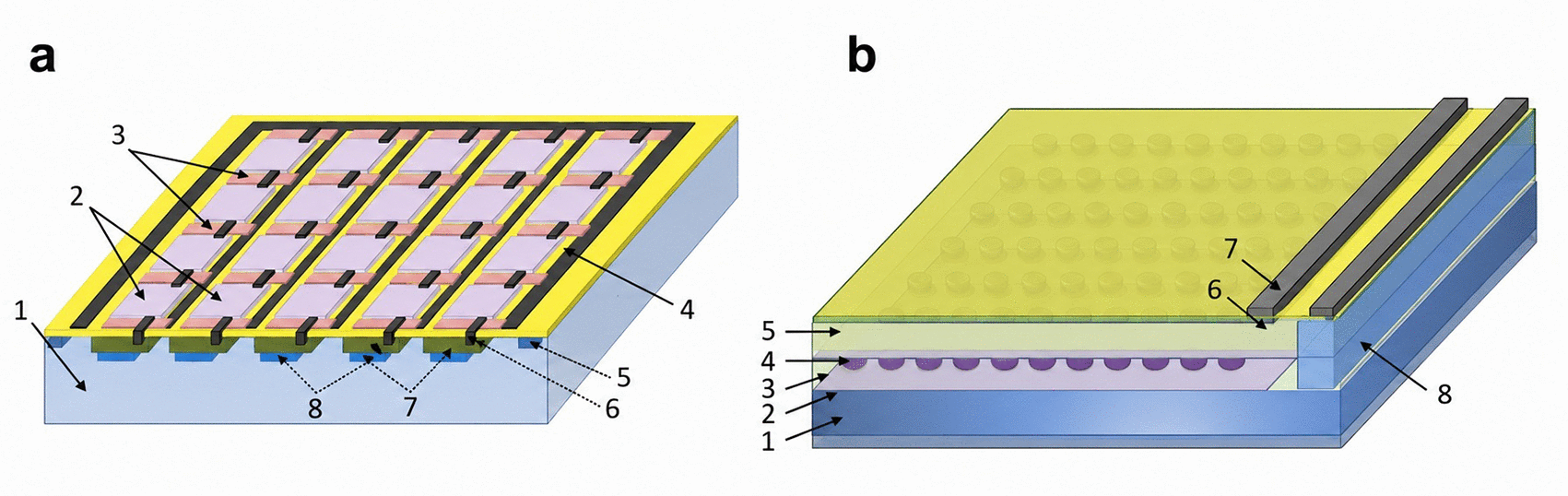
Figure 2. (a) Structure of the conventional surface-pixel SiPM (MPPC S12572-010P). (b) Structure of the buried-pixel SiPM (MAPD-3NM-II).
Figure 2. SiPM with surface pixel structure (a) and buried pixel structure (b).
In contrast, the developed buried pixel structure employs a deep-substrate architecture,11–16 where the avalanche multiplication region is embedded beneath a transparent, passivated top layer, eliminating the need for direct metal contact in the active detection zone. This design significantly increases the effective fill factor (100%), and enhances the PDE by reducing surface optical dead zones. The deeper electric field geometry also helps to improve uniformity of gain and timing resolution across the micro-pixel array. To address the inherent limitations of surface-pixel SiPM architectures, a proposed buried pixel detector design has been developed, as shown in
Figure 2b (Model MAPD-3NMII). This advanced structure begins with a high-purity silicon substrate 1, selected based on its conductivity type and grown using the Czochralski or float-zone method to ensure structural uniformity and minimal defect density. The device incorporates an n-type layer 2 as the base, which plays a critical role in defining the electric field distribution and supporting the charge collection from the multiplication region. Above this lies the first p-type epitaxial layer 3, which is essential for forming the buried junction and guiding the avalanche process away from the surface, thereby improving detection uniformity and reducing surface-related noise. The pixel 4 in this architecture is notably smaller—10 μm—allowing for higher spatial resolution and improved fill factor within a densely packed array. A second p-type epitaxial layer 5 is introduced to fine-tune the vertical electric field profile and enhance the avalanche confinement deep within the substrate. This dual-epitaxy structure not only boosts the PDE by maximizing the active volume but also improves gain uniformity across the device. The contact area 6 is designed to ensure efficient biasing without obstructing incident photons, while aluminum contacts 7 are used to establish electrical connectivity with external circuits, selected for their compatibility with CMOS integration and excellent conductivity. To mitigate edge-related electrical stress and suppress premature breakdown phenomena, a guard ring 8 is incorporated at the periphery of the detector. This structural feature ensures stable high-voltage operation and extends the breakdown threshold of the device, making it suitable for high-gain, low-noise applications in precision photon counting.
The breakdown voltage (Ubreak) is a key parameter for each SiPM and must be accurately defined (
Figure 3). This was achieved by calculating the derivative of the current J with respect to voltage U, normalized by the current itself, as expressed by the following expression
. The breakdown voltage was defined as the voltage corresponding to the maximum value of the rate of change of the current.
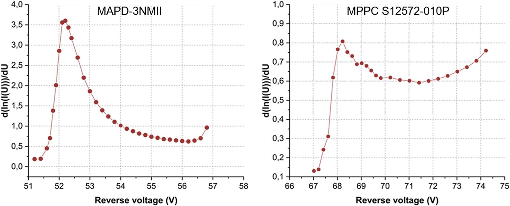
Figure 3. Determination of the breakdown voltage from the normalized current derivative.
Figure 3. Determination of breakdown voltages.
Figure 4 illustrates the dependence of the internal gain on the applied reverse voltage for the MPPC S12572-010P (left) and the MAPD 3NM-II (right) measured at room temperature (~23 °C). The internal gain M at various reverse voltages was determined using the following equation:
where C
pixel - pixel capacitance, Uapp.v - the applied voltage (U
oper ⩾ U
break), U
break - the breakdown voltage, m - coefficient which may change from 1 to 2 depending on the values of resistance of the depletion layer and the capacitance of the pixel, G
am - the amplification coefficient of the amplifier or preamplifier (100 times), q - electron charge and A
average- the corresponding ADC channel number (40fC charge per chanel) to the amplitude of a single photoelectron. A linear increase in gain with increasing reverse voltage is observed. The extrapolated intersection of the linear fit with the voltage axis, corresponding to a gain approaching zero, was identified as the breakdown voltage (U
oper ≈ U
break). The breakdown voltages obtained from the gain analysis are close in value, amounting to approximately 52.3 V for the MAPD 3NM-II and 68 V for the MPPC S12572-010P.
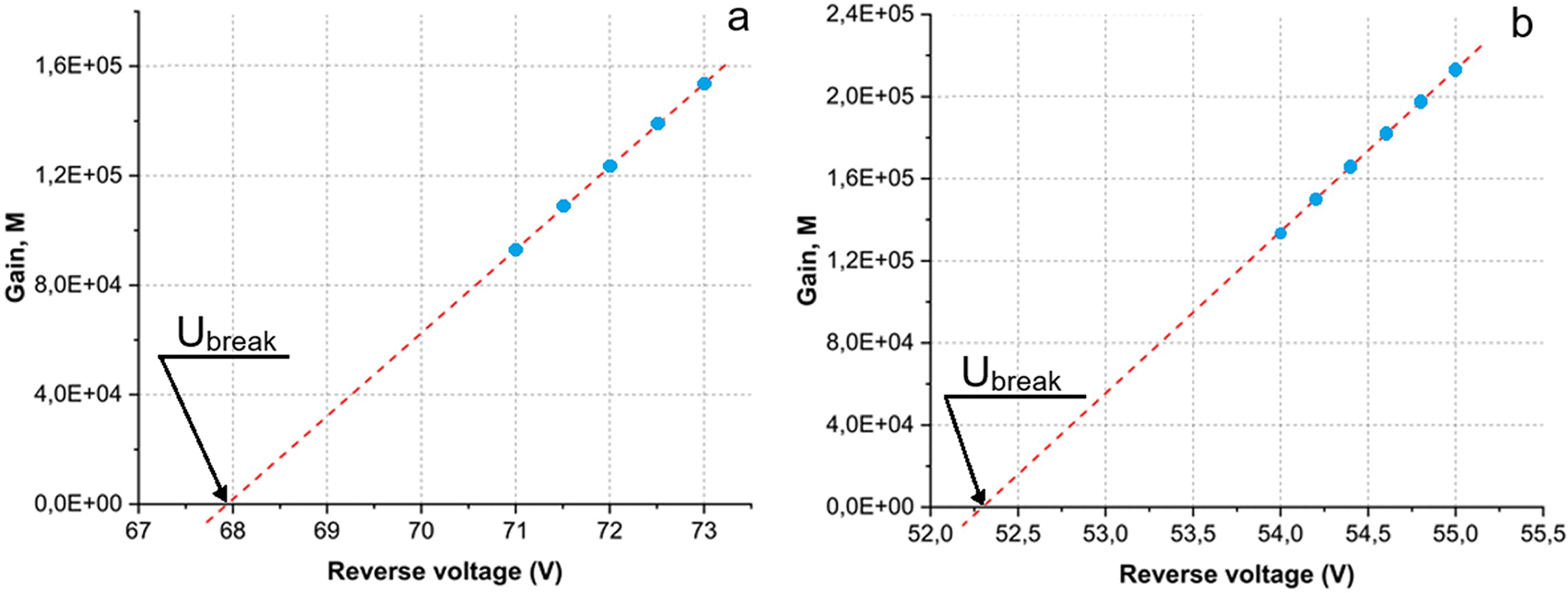
Figure 4. Dependence of the internal gain on the applied reverse voltage for the MPPC S12572-010P and MAPD-3NM-II measured at room temperature.
Figure 4. The dependence of the gain on the applied voltage for MPPC-S12572-010P (left) and MAPD 3NM-II (right) at room temperature (~23 °C).
The photon detection efficiency of the MAPD-3NM-II photodiode and the MPPC S12572-010P was evaluated using a pulsed single-photon counting technique. The measurements were performed with a pulsed green laser source operating at a wavelength of 530 nm. Accurate application of the single-photon counting approach requires sufficient pedestal statistics. At low overvoltage values (approximately 1 V), the method becomes unreliable due to broadening of the pedestal peak, whereas at high overvoltages (around 5 V), increased dark count rates and optical cross-talk significantly distort the spectra. For this reason, PDE measurements were conducted at intermediate overvoltages.
A comparative analysis of the PDE was carried out under two different conditions: identical applied overvoltage and identical internal gain. The pulse-height spectra recorded at an overvoltage of 4 V and at a gain close to 105 in Fig. 5. In all cases, the mean number of photons per pulse incident on the active area of both detectors was maintained at the same level. At an overvoltage of 4 V, the internal gain of the MAPD-3NM-II reached 1.2*105, while the MPPC S12572-010P exhibited a gain of 8.5 × 10⁴. Under identical overvoltage conditions, the PDE was found to be 32% for the MAPD-3NM-II and 8% for the MPPC S12572-010P. When comparing the detectors at equal gain, the PDE of the MPPC increased to 9.5%, whereas the MAPD-3NM-II maintained a value of 32%. This substantial discrepancy is mainly attributed to differences in the geometrical fill factor: approximately 33% for the S12572-010P and 100% for the MAPD-3NM-II.
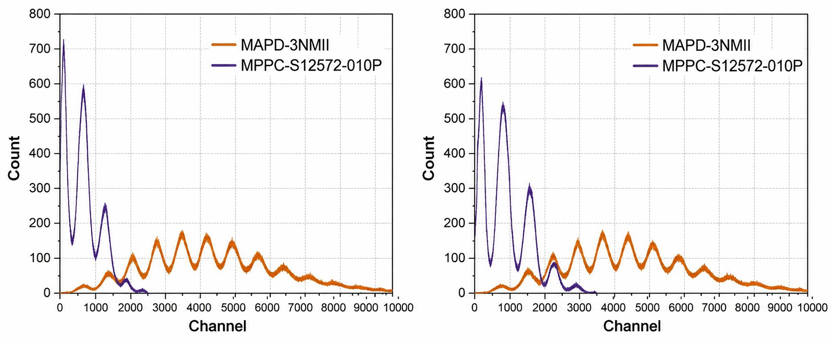
Figure 5. Pulse height distribution of surface pixel (MPPC-S12572-010P) and buried pixel (MAPD-3NMII) structures at same overvoltage of 4 V (left) and at same internal gain (right).
Figure 5. Pulse-height distributions of the surface-pixel (MPPC S12572-010P) and buried-pixel (MAPD-3NM-II) structures at the same overvoltage of 4 V (left) and at the same internal gain (right).
Conclusion
The integration of silicon photomultipliers (SiPMs) into bathymetric LIDAR systems represents a significant advancement in underwater topographic mapping, offering enhanced sensitivity, photon detection efficiency, and spatial resolution. Traditional surface-pixel SiPMs, while effective, are constrained by lower fill factors, limited dynamic range. In contrast, the newly developed buried pixel SiPM architecture, demonstrates clear advantages in photon-counting performance, linearity, and robustness under low-light aquatic conditions.
Spectral analyses confirm the superior photon resolution of buried pixel devices, exhibiting well-defined multi-photon peaks (up to 10 or more) in charge histograms—compared to the 5 peaks typically observed in surface-pixel designs. This enhancement is directly attributable to increased fill factor, improved avalanche confinement, and optimized field uniformity. These features make the buried structure particularly well-suited for integration into compact, drone-mounted LIDAR systems that require both mechanical durability and ultra-low photon threshold detection.
In conclusion, buried pixel SiPM technology offers a transformative solution for advancing LIDAR-based bathymetry, addressing longstanding challenges in photodetector efficiency, resolution, and environmental adaptability. Continued development and optimization of this architecture are expected to drive significant progress in photon-counting instrumentation for marine science and remote sensing.
Ethics and consent
Ethical approval and consent were not required for this study because no human participants, animals, or personal data were involved.