1. Introduction
Micro-pixel avalanche photodiodes (MAPDs), also known as silicon photo-multipliers (SiPMs), have become one of the most promising semiconductor photo-detectors for modern radiation detection systems due to their compact dimensions, high internal gain, low operating voltage, immunity to magnetic fields, and compatibility with scintillation materials.1–5 These devices are widely used in high-energy physics experiments, nuclear instrumentation, positron emission tomography (PET), radiation monitoring systems, astrophysical experiments, and fast timing applications.6–11 Despite the rapid development of SiPM technologies, conventional structures still suffer from several important limitations, including long recovery time, dead-space losses associated with surface quenching resistors, limited PDE, and saturation effects under high particle flux conditions.12–15 Inactive regions significantly reduce the geometrical fill factor and therefore limit the effective photosensitive area of the detector.16–20
Several approaches have previously been proposed to improve the PDE and timing characteristics of silicon photo-multipliers, including optimization of pixel geometry, avalanche multiplication regions, and anti-reflection coatings.21–26 However, achieving simultaneously high PDE, ultra-fast recovery time, and high pixel density remains a major challenge in semiconductor detector technology.
The main objective of the present study was the development of novel MAPD structures capable of simultaneously improving PDE and detector recovery dynamics. In this work, two new MAPD structures based on field-induced potential micro-wells and field-induced micro-resistor structures were proposed and experimentally investigated.
2. Methods
The proposed MAPD structure was shwon in
Figure 1. A sequence of n-type and p-type epitaxial layers with resistivities of 250 Ω·cm and 20 Ω·cm, respectively, was grown on an n-type silicon substrate possessing a resistivity of 20 Ω·cm. The thicknesses of the n-type and p-type epitaxial layers were selected as 4 μm and 7 μm, respectively. To improve electric-field uniformity near the substrate surface, a thin highly doped n+-type layer was formed using arsenic implantation. Highly doped n+-type pixels were subsequently created between the epitaxial layers. Depending on the intended application, the pixel diameter varied between 5 and 10 μm, while the spacing between neighboring pixels ranged between 3 and 5 μm. Such geometry allowed the pixel density to reach approximately 4×104 pixels/mm2. The increase in pixel density significantly expanded the linear dynamic range of the photodiode response under intense photon flux conditions. Unlike conventional SiPM structures containing inactive regions occupied by quenching resistors and isolation structures, the proposed MAPD structure provides nearly complete photosensitive surface coverage.
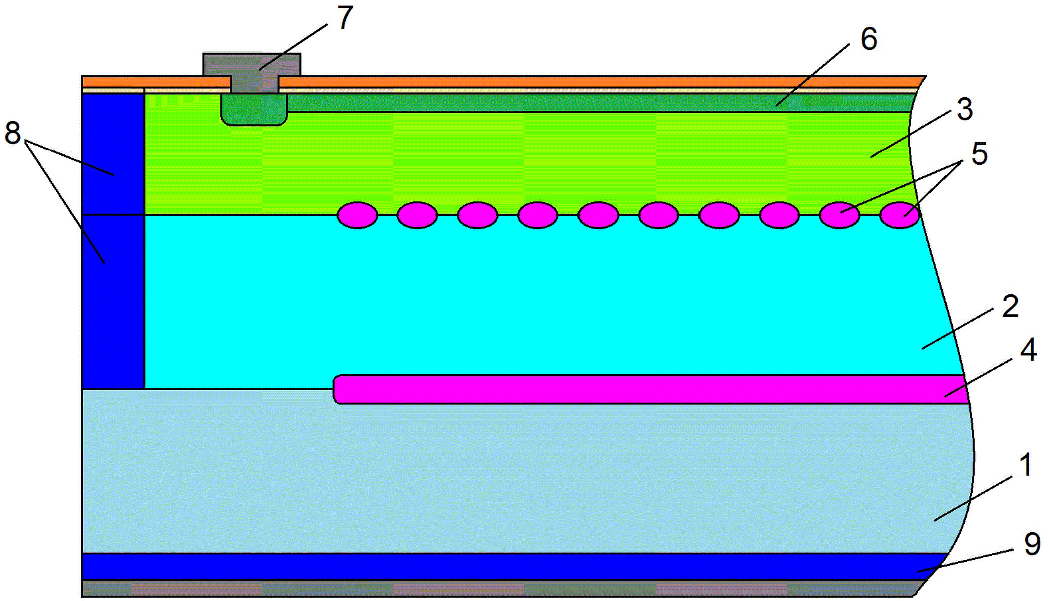
Figure 1. General structure of the proposed MAPD structure.
1 – n-type silicon substrate; 2 – n-type epitaxial layer; 3 – p-type epitaxial layer; 4 – thin n+-type layer; 5 – matrix of n+-type regions (pixels); 6 – p+-type layer; 7 – metal contact; 8 – n+-type guard ring; 9 – n+-type conductive layer (back contact).
In order to further improve detector recovery dynamics, a second MAPD structure based on a field-induced micro-resistor structure was developed. The structure and operating principle of the proposed micro-resistor MAPD are illustrated in
Figure 2. Under operating conditions, a reverse bias voltage was applied to the MAPD structure. As a result, a depletion region formed at the interface between the p-type and n-type epitaxial layers. The presence of highly doped n+-type pixels significantly modified the electric-field distribution inside the structure. At sufficiently small pixel spacing, the electric field penetrated into the n-type epitaxial layer, resulting in the formation of artificial potential micro-wells. The avalanche multiplication process occurred at the interface between the highly doped n+-type pixels and the p-type epitaxial layer similarly to conventional Geiger-mode avalanche photodiodes.26,27 Electrons generated by incident photons accumulated inside the micro-wells and partially screened the electric field in the avalanche region. Subsequently, the accumulated electrons drifted into the substrate volume, restoring the electric field in the pixel region. However, the charge evacuation process in such structures remained relatively slow, resulting in recovery times approaching 300 μs.
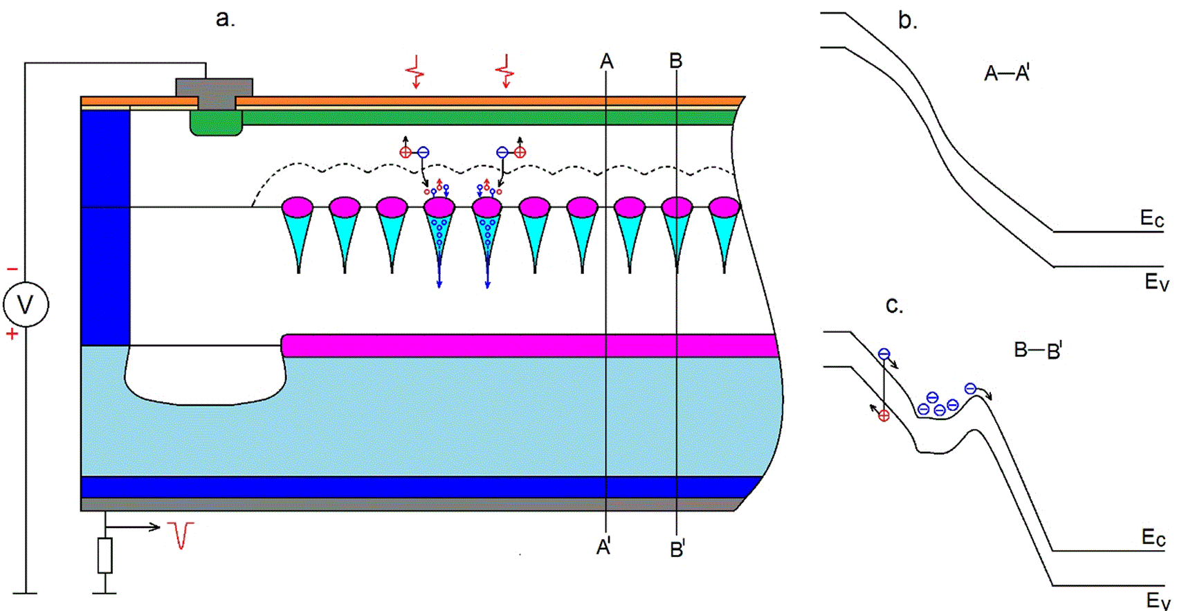
Figure 2. Potential micro-well MAPD and corresponding energy diagrams.
Although the recovery time was relatively large, the proposed structures demonstrated several important advantages, including high PDE, high fill factor, and high pixel density. Therefore, these devices could successfully operate in low particle flux systems up to approximately 3 × 10³ particles/s.
One of the principal limitations of conventional SiPMs is the relatively long recovery time caused by parasitic RC effects and slow charge evacuation from avalanche regions.26,27 In addition, the presence of inactive dead zones reduces the geometrical fill factor and limits the PDE. To overcome these limitations, a novel micro-channel MAPD structure was proposed (see Figure 3). The spacing between neighboring highly doped n+-type pixels was reduced to approximately 2 μm. Such geometry prevented the merging of depletion regions inside the n-type epitaxial layer. As a result, each pixel became connected to the substrate through a thin conductive micro-channel acting as an intrinsic micro-resistor. The resistance of the micro-channel can be expressed as:
where:
• ρ = 250 Ω·cm is the resistivity of the micro-channel,
• Wn = 7 μm is the depletion-region thickness,
• dm = 5 μm is the micro-channel diameter.
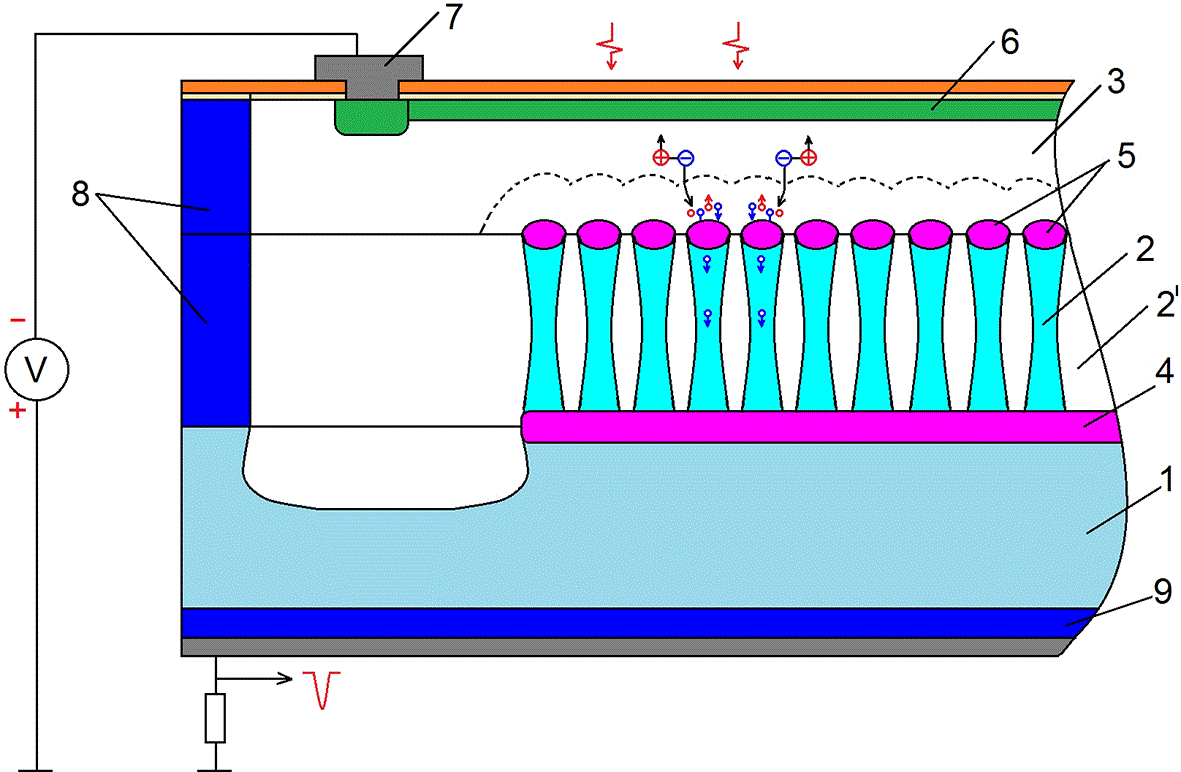
Figure 3. Proposed micro-channel MAPD structure.
Since potential micro-wells were not formed in this structure, the recovery time was determined by the RC constant of the micro-channel and pixel capacitance:
The proposed structure provides several important advantages over conventional MAPDs:
• elimination of dead regions,
• reduced parasitic capacitance,
• improved electric-field uniformity,
• ultra-fast charge evacuation,
• enhanced PDE,
• higher count-rate capability.
Experimental investigations demonstrated that the recovery time was reduced from approximately 300 μs to 40 ns. Such reduction dramatically increased the detector count-rate capability up to approximately 107 particles/s.
3. Experimental
Capacitance is one of the most important parameters of avalanche photodiodes because it allows determination of the depletion voltage, active-region thickness, and dopant concentration profile. The capacitance-voltage characteristics of the developed MAPDs were investigated using a differential RC electrical circuit similarly to standard semiconductor detector characterization methods (see Figure 4). A sinusoidal signal generated by a Tektronix AFG 3101C pulse generator was applied to the diode through a 47 nF capacitor. A 50 Ω grounding resistor and a 7.5 kΩ protective resistor were employed in the circuit. The reverse bias voltage was supplied using a Keithley 6487 Picoammeter/Voltage Source, which additionally enabled dark-current measurements. Signal amplitudes were measured using a Hantek DSO 5202B digital oscilloscope. The diode capacitance was calculated according to:
where:
• Ce is the reference capacitance,
• Cd is the photodiode capacitance,
• Ae is the signal amplitude from the reference capacitor,
• Ad is the signal amplitude measured from the photodiode.
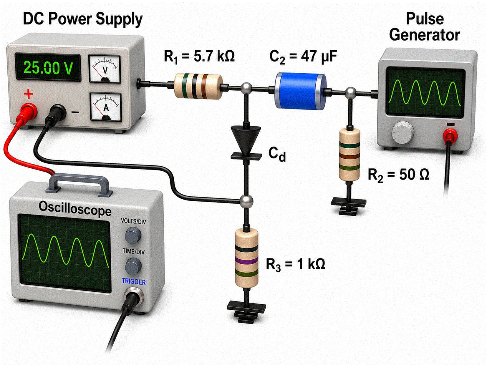
Figure 4. Experimental setup used for capacitance measurements.
4. Results and discussion
4.1 Capacitance-voltage characteristics
The measured capacitance-voltage characteristics was shown in
Figure 5. It demonstrated that the capacitance decreased with increasing reverse bias voltage. A sharp decrease in capacitance corresponded to rapid variations in dopant concentration inside the active region. At sufficiently high voltages, the capacitance approached saturation, indicating complete depletion of the active region. The depletion voltages differed among the investigated MAPDs. For MAPD-3 N, complete depletion occurred near 20 V, while for MAPD-K0 the corresponding voltage approached approximately 22 V. For the remaining devices, depletion voltages were close to 30 V.
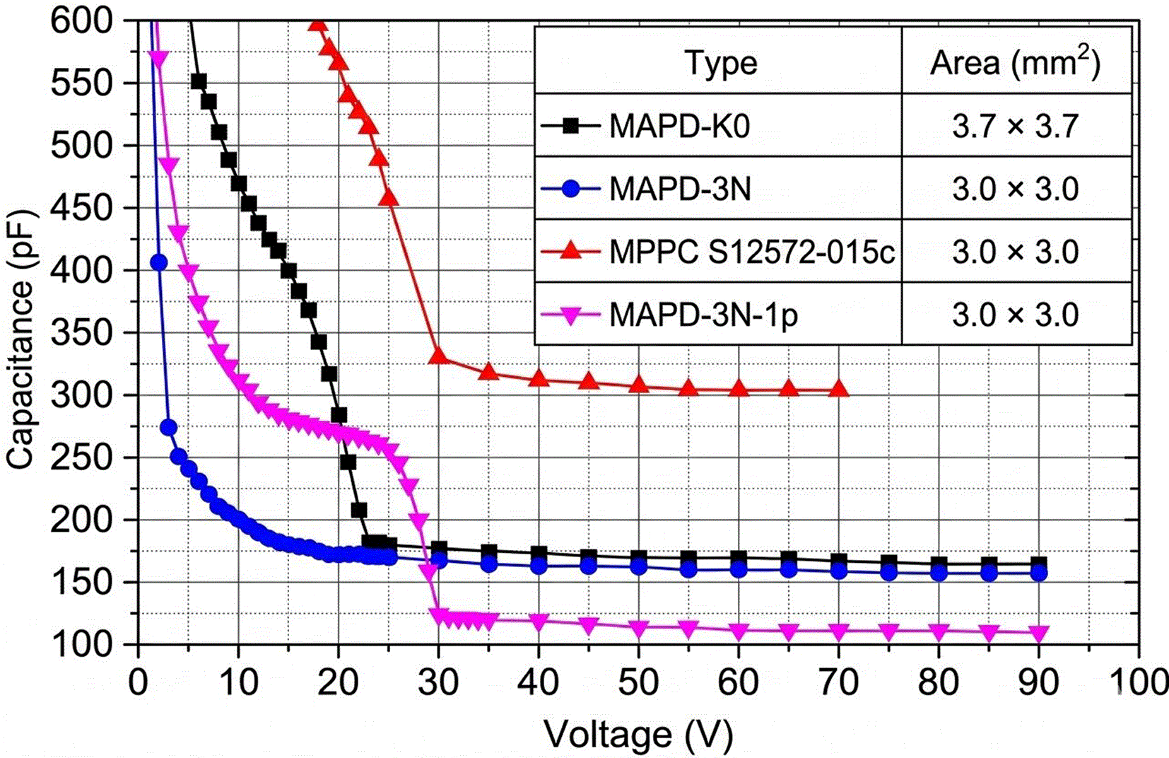
Figure 5. Capacitance-voltage characteristics of different MAPDs.
4.2 Enhancement of PDE
PDE of silicon photomultipliers is determined by three principal factors: the quantum efficiency (QE), the avalanche triggering probability (P), and the geometrical fill factor (FF). Consequently, improvements in any of these parameters directly contribute to enhanced detector sensitivity. To maximize the quantum efficiency, anti-reflection dielectric coatings based on silicon nitride (Si3N4) and silicon dioxide (SiO2) were deposited on the photosensitive surface of the developed MAPDs. Optimization of the coating thickness significantly reduced optical reflection losses and increased the quantum efficiency to approximately 85% within the spectral region of interest. Similar approaches have previously been shown to enhance photon absorption in silicon photodetectors. An additional contribution to PDE enhancement originates from the proposed device architecture itself. Unlike conventional SiPM structures that contain inactive regions associated with quenching resistors and isolation elements, the developed MAPDs exhibit an almost fully photosensitive surface. The elimination of dead areas increases the geometrical fill factor and consequently raises the probability that incident photons generate photoelectrons within active avalanche regions. Furthermore, the optimized electric-field
distribution in the buried multiplication region improves avalanche triggering efficiency, thereby increasing the probability that a single photoelectron initiates a detectable avalanche event. As a result of these combined improvements, the photon detection efficiency of the developed MAPDs reached approximately 40%, representing a significant enhancement compared with conventional MAPD and SiPM devices operating with similar pixel densities.
The influence of pixel geometry on PDE is illustrated in
Figure 6. The results demonstrate an approximately linear increase in PDE with increasing pixel area. Larger pixels provide a greater active multiplication region and a higher geometrical fill factor, leading to an increased probability of photon conversion and avalanche initiation. Based on this dependence, the pixel diameter in the MAPD-3 K structures was increased to approximately 7 μm, resulting in a PDE of about 40%.
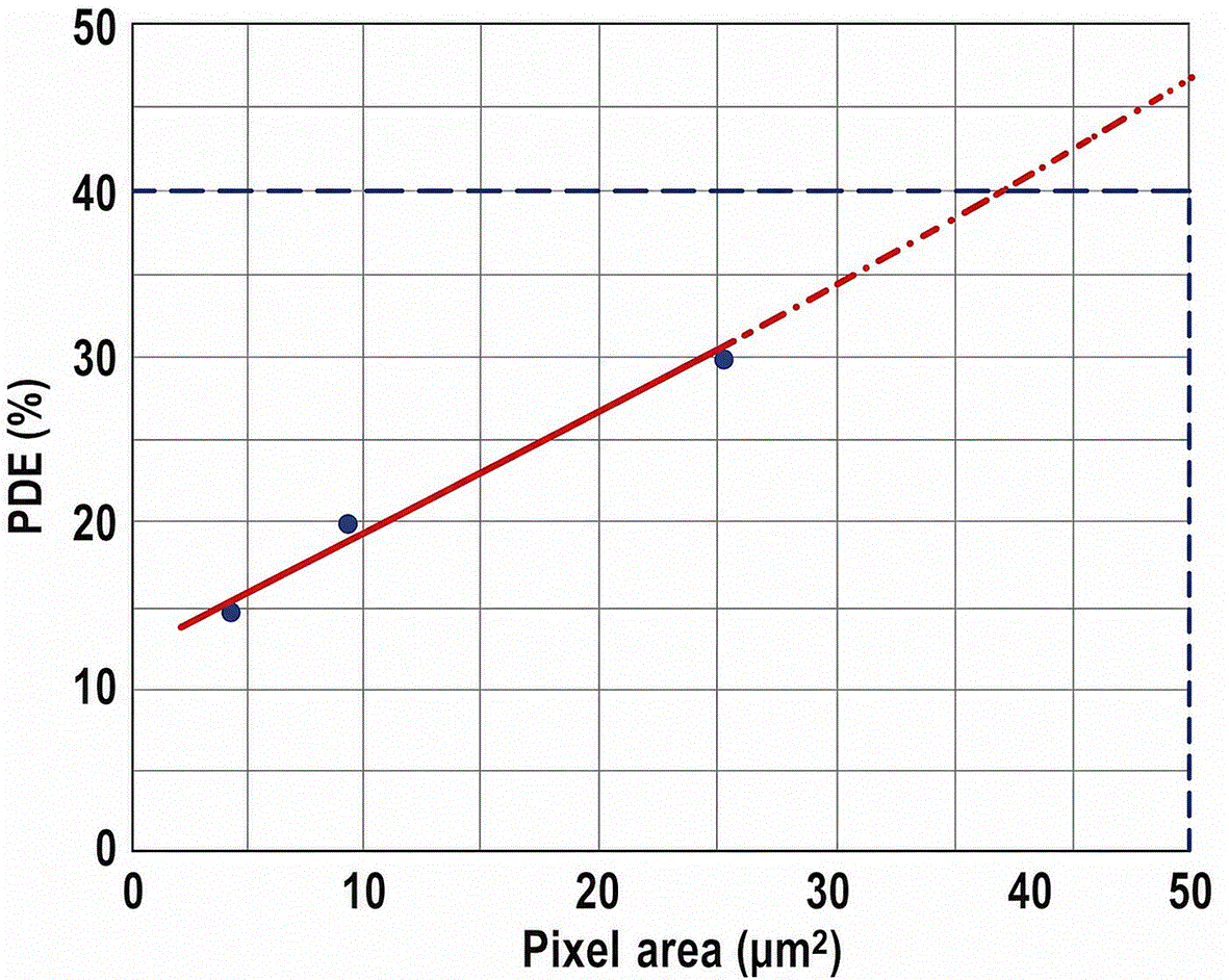
Figure 6. Dependence of PDE on pixel area.
The observed relationship between pixel area and PDE suggests that further optimization of pixel geometry remains an effective approach for improving detector sensitivity. However, increasing pixel dimensions must be balanced against the associated reduction in pixel density and dynamic range. Therefore, the selected pixel size represents a compromise between achieving high photon detection efficiency and maintaining the high-rate performance required for modern radiation detection applications.
5. Conclusion
Novel high-efficiency MAPD structures employing artificial potential micro-wells and intrinsic micro-channel recovery mechanisms were successfully developed and experimentally investigated. The obtained results demonstrated that optimized electric-field engineering and ultrafast charge evacuation mechanisms significantly improve both the photon detection efficiency and recovery dynamics of silicon photo-detectors.
The developed MAPDs provided nearly 100% photosensitive surface coverage, high pixel density, enhanced PDE, and substantially improved high-rate performance. Experimental investigations showed that the recovery time was reduced from approximately 300 μs to 40 ns, while the PDE reached approximately 40%. In addition, the elimination of inactive dead regions significantly increased the geometrical fill factor and improved avalanche triggering probability.
Due to the combination of high PDE, fast recovery time, and high pixel density, the proposed MAPDs are highly promising for applications requiring fast and efficient photon detection under high counting-rate conditions. The developed structures can potentially be used in time-of-flight positron emission tomography (TOF-PET) systems, high-energy physics detectors, Cherenkov detectors, scintillation detectors, neutron detection systems, calorimeters, space radiation monitoring systems, homeland security technologies, LiDAR systems, and various fast timing applications.
The proposed structure is particularly attractive for detector systems operating under high particle flux conditions where conventional MAPDs experience saturation effects and performance degradation. Therefore, the obtained results demonstrate that the proposed MAPD structures represent a promising direction for the development of next-generation high-speed silicon photo-detectors intended for advanced scientific, medical, and industrial applications.
Ethics and consent
Ethical approval and consent were not required for this study because no human participants, human tissues, personal data, or experimental animals were involved.