Ensuring protection of key transistors from overload
Metal oxide semiconductor field effect transistors (MOSFET), insulated gate bipolar transistors (IGBT), and silicon carbide (SiC) transistors are the main types of transistors used in switching nodes. These transistors are sensitive to overloads and short circuit currents, which can lead to their failure if not adequately protected.
Failure typically occurs when these transistors overheat above 150°C or when they exceed the maximum impulse collector current (ICM), which operates for a very short but excessive duration for this type of transistor. Consequently, reliable protection mechanisms are essential during emergency conditions.
The methods and implementation of protection are determined by the requirements of the Safe Operating Area (SOA) specific to each transistor type. The protective hardware or system must promptly detect any deviations from normal operation, limit current overload conditions, and transition the transistors to a non-conducting state in the event of a short circuit.
It is important to distinguish between an overload condition (OC), where the current does not exceed twice the permissible operating value, and a short circuit current (SC), where the current can exceed the permissible value by several times or more.
Unlike short-circuit currents, overload currents do not cause immediate failure of the key transistors. The overload mode is characterized by a relatively gradual temperature increase in the transistors. This is due to the nature of high-voltage pulsed action on biomass, where the maximum pulse current (Imax) gradually increases as a function of the number of pulses (N) applied to the electroporated biomass (Imax = f(N)). Without proper limitation of the power dissipated by the key transistors, this temperature increase can reach critical levels.
The critical temperature limit is determined by the maximum allowable power (Ptm) that can be dissipated by the key transistors. This power value is determined either through computational methods or experimental analysis and depends on the specific transistor type and cooling conditions.
Limiting the rise in temperature of key transistors, when it occurs due to excessive power dissipated on them, is possible with the help of software control of the pulse repetition rate. To implement this regulation, the current value of the power dissipated by the key transistors is continuously calculated during the interval between pulses. This power dissipation is a component of the total power dissipated in the discharge circuit.
The total power dissipated (PDC) in the discharge circuit during electroporation is determined every second as the sum of the energy released during this time by all pulses applied to the electroporated biomass as shown in Equation 1:
Where N is the number of pulses delivered in 1 sec and Wi is the energy dissipated in the discharge circuit by one pulse defined in Equation 2:
where CESC is the ESC capacitance,
UIV is the initialization voltage value (initial voltage of the pulse),
URV is the residual voltage of the pulse.
This calculation requires a voltage measurement across the ESC before (UIV) and after (URV) each pulse.
During the pulse action, it is important to note that the ESC does not get charged.
The total power dissipated during the discharge is determined by the expression shown in Equation 3:
where F is the pulse repetition frequency.
The total resistance of the discharge circuit is calculated after each pulse using the following Equation 4
where ti is the pulse duration.
The total resistance of the discharge circuit, Equation 5, is the sum of the biomass resistance (RBM), of resistance equalization resistors (RER) and resistance of fully conductive key transistors (RKT).
In this case, the power dissipated by the key transistors (PKT), Equation 6, is proportional to the ratio of the resistance of fully conducting and parallel-connected key transistors (RKT) to the total resistance of the discharge circuit (RDC).
If the power dissipated by the switching key transistors (PKT) exceeds the maximum allowable power dissipation (Ptm), the pulse repetition frequency (F) is decreased according to Equation 7:
The pulse repetition frequency is chosen as a regulating factor for the parametric response to overload of the key transistors. This choice is based on two main considerations. First, linear dependence: The dissipated power in the key transistors exhibits a linear relationship with the pulse repetition frequency. By decreasing the pulse repetition frequency, the power dissipation can be effectively reduced. This linear dependence allows for a straightforward and predictable adjustment of the system to manage the power dissipation within acceptable limits. Second: minimal impact on biomass electroporation qualitative indicators: Among the various parameters involved in the electroporation process, the pulse repetition frequency has been observed to have a lesser impact on the qualitative indicators of electroporation. This means that adjusting the pulse repetition frequency to address the overload of key transistors does not significantly compromise the overall effectiveness and quality of the electroporation process. Therefore, it can be considered a suitable parameter for regulation without compromising the desired outcome. Thus, by incorporating the pulse repetition frequency as a control parameter, it is possible to maintain the safe operation of the key transistors by effectively managing their power dissipation levels, while ensuring the overall success and quality of the electroporation process.
It should be noted that microcontroller-controlled variability of the pulse repetition frequency as a regulating factor in the parametric response to overload of key transistors is necessary, first of all, for universal devices that are used for electroporation of various types of biomass and for which performance is not a critical parameter. Such devices are used in small agricultural associations for the disposal of production waste (tops or substandard fruits and vegetables, for example), as well as for the disposal of relatively small volumes of waste from food industry enterprises. Performance, as a determining parameter, is also not important for laboratory devices. Microcontroller-controlled pulse repetition rate variability is less necessary when using HVPG for a single biomass species with predictable conductivity. Such devices are used for large industries where productivity is a critical indicator (sugar beet processing, for example).
Ensuring protection of key transistors from short circuit current
In addition to its higher amplitude compared to overload currents, the short-circuit current stands out for its sudden and unpredictable nature. This current determines the unacceptably high power dissipated on the key transistors, which leads to their failure. Therefore, the development of a switching node with effective protection against short-circuit currents is a critical stage in the design of a high-voltage pulse generator.
The process of building a switching node involves developing methods, electrical circuits, and selecting components that provide protection for key transistors against potential short-circuit currents. These currents can occur during electrical breakdown of biomass, during accidental direct contact of a movable electrode with a stationary one in a press electrode device, or when a metal particle enters the interelectrode space in flow electroporation devices.
There are autonomous and systemic methods for protecting key transistors from short-circuit currents. The autonomous method involves using specialized drivers for IGBT transistors with an additional protective function. These drivers are designed to terminate the short-circuit mode within a duration of 1 to 10 microseconds. The transistor, controlled by such a driver, must withstand the short-circuit current during this period.
In drivers with short-circuit protection, there is a dedicated Current Sense Input (CS) that is connected to either the current measuring resistor (referred as RSENSE) in the emitter circuit or the collector of the transistor, using additional resistive-capacitive measuring circuits. In the first case, the driver monitors the transistor's current, while in the second case, it monitors the transistor's saturation voltage. If the current exceeds the acceptable limit, the driver switches the transistor to a non-conducting state. The protection is disabled when the input signal is removed.
The advantages of using short-circuit current protection with specialized drivers include: 1) improved efficiency of the switching node by using low-resistance RSENSE resistors in the emitter circuits or eliminating them altogether with saturation current control, and 2) relative simplicity in implementing the protection circuit, as it only requires one active element - the driver.
However, there are some disadvantages to consider when using specialized drivers in biomass electroporation devices: 1) difficulties in selecting RSENSE measuring resistors suitable for high load currents and short circuits currents, 2) challenges in choosing drivers due to their compatibility with specific transistor parameters, 3) parametric load instability and current surges that may hinder accurate detection of the short-circuit mode by the driver, 4) limited availability of drivers with a wide range of parameters suitable for devices operating at voltages over 1000 Volts, 5) lack of a built-in function to trigger an output signal from the driver to halt the microcontroller's control pulses in the event of a short circuit, and 6) complexity of application when parallel connection of key transistors is required or the use of specialized switching modules with no short circuit protection.
The systemic method of short circuit protection offers an alternative approach to the autonomous method by primarily utilizing existing hardware as system resources for this purpose.
When dealing with a low-resistance and unstable load, such as biomass, the first challenge to address is the delineation of the maximum load and short circuit modes. The discharge of high-voltage energy from an energy-storage capacitor to a low-resistance load creates a blurred boundary when distinguishing between these two modes. This issue is further complicated by the occurrence of current surges in most cases, as illustrated in Figure 1. These surges result from the resonance of reactive components within the discharge circuits. In fact, the magnitude of the current surge can exceed two or more times the maximum value of the pulse itself.
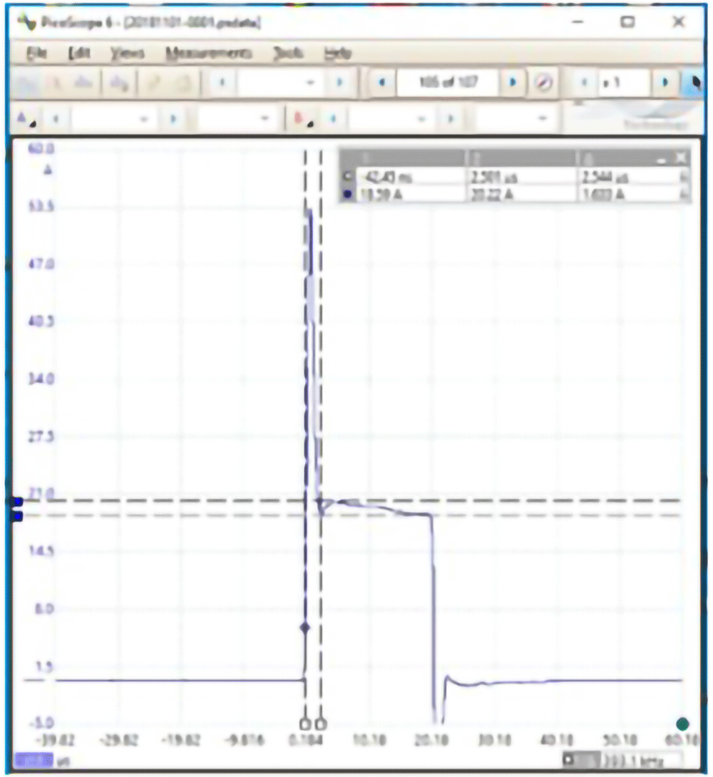
Figure 1. Sample current form for a single pulse during electroporation of a low-resistance green seaweed Ulva sp. biomass8,14.
Determining the boundary between maximum load current and short circuit current is a crucial task in developing switching nodes for high-voltage pulse generators. This boundary depends on two key factors. Firstly, it is determined by the maximum permissible current for the selected key transistors' semiconductor structure, considering the allowable duration of this current. Secondly, the boundary is influenced by the discharge level of the energy storage capacitor (ESC) during the pulse duration. In the event of a short circuit, which typically occurs when a subsequent pulse is applied to the load, there is a sudden and excessively rapid drop in the charging voltage of the ESC. This mode of operation can be problematic and needs to be addressed to ensure safe and reliable performance.
During normal operation, it is acceptable for the initialization voltage on the energy storage capacitor (ESC) to decrease by up to 37% during the specified duration of one pulse. However, if the voltage drop on the ESC exceeds 37% of the initialization voltage when the current pulse is applied, it indicates an abnormal condition. In such cases, it is necessary to terminate the action of the current and subsequent pulses to prevent any potential damage or failure. The determination of this boundary can be achieved through a combination of hardware and software measures. By implementing appropriate hardware design, such as selecting key transistors with suitable current ratings and incorporating protective components, the maximum load current and short circuit current can be effectively managed. Furthermore, software algorithms can be developed to continuously monitor the voltage drop on the ESC during pulse application the termination of the current and subsequent pulses is carried out.
In Figure 2, we present an illustrative circuit diagram of a switching node that we have designed. This circuit incorporates a safeguard mechanism against short-circuit currents. What sets it apart from commonly employed schematics for building similar nodes is the incorporation of supplementary elements, namely the COMP comparator and the low-power MOSFET transistor Q3.
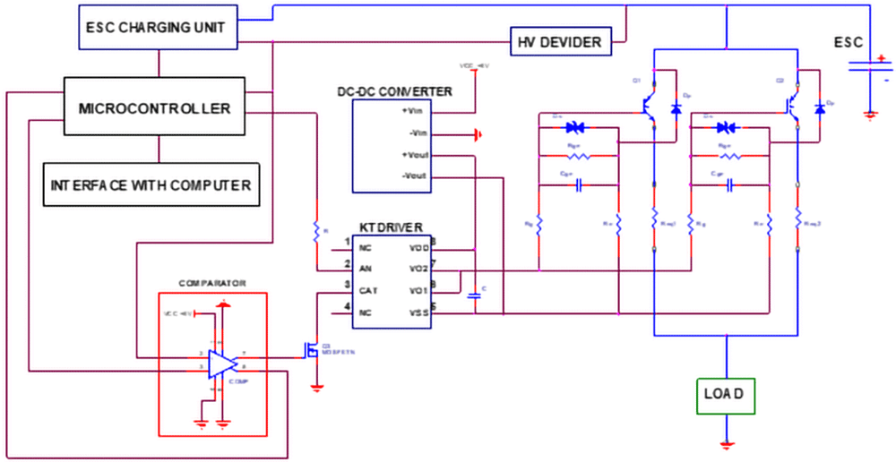
Figure 2. The electrical circuit diagram of the switching node with its implemented system protection against short-circuit current.
The developed switching node is based on a schematic that incorporates two key IGBT transistors, Q1 and Q2, connected in parallel with equalization resistors (Req1, Req2) in their emitter circuits. Both transistors are connected to the load, labeled as "LOAD," through these equalization resistors. The series connection of the energy-storage capacitor (ESC), key transistors, equalization resistors, and the load forms the discharge circuit. The control of the key transistors is achieved using the key transistor driver, denoted as "KT DRIVER," with special connection circuits connecting its output to the gates of the controlled transistors.
Power for the driver and its circuits is provided by an isolating DC-DC converter called the "DC-DC CONVERTER." The voltage on the ESC is measured using a voltage divider labeled as "HV DEVIDER." The voltage measured at the ESC output of the divider is then fed to the analog-to-digital converter of the microcontroller for ADC conversion, evaluation, storage, and display purposes. Additionally, the measured voltage from the divider output is used as a negative feedback factor for regulating the ESC charging unit, labeled as "ESC CHARGING UNIT," and is also fed directly to the input of the comparator, labeled as "COMPARATOR," for qualitative assessment of the voltage drop level on the ESC. The inverted input of the comparator is connected to the microcontroller's digital-to-analog converter (DAC) output, where a comparison voltage is set to represent the permissible boundary level of voltage drop on the ESC.
Control pulses for key transistors Q1 and Q2 are generated by the microcontroller and supplied to the input of the driver "KT DRIVER" through one of its digital outputs.
When the load current is within the permissible range, transistor switch Q3 remains conductive and allows the control pulses to pass through.
The essence of the current protection, as proposed in this schematic, is that in the event of a short circuit, the control pulse from the microcontroller is interrupted by transitioning the key Q3 to a non-conductive state.
The conductivity of the Q3 key is controlled by the comparator "COMPARATOR", the output of which is connected to the gate of the Q3 key. When pulses are applied to an allowable load, the charge voltage drop across the ESC (called the initialization voltage) must not exceed a predetermined limit, which is calculated by the microcontroller. The microcontroller calculates the value of the initialization voltage drop based on the specified values of this voltage, the pulse duration and the minimum allowable resistance of the discharge circuit.
The minimum allowable resistance value (RDC, Equation 8) of the discharge circuit is determined by the ratio of the maximum initialization voltage (UIV = Umax) to the maximum allowable pulse current (Imax):
The result of this calculation is the value of the residual voltage, which is set as a comparison signal by the microcontroller at the inverse input of the comarator "COMPARATOR".
The microcontroller calculates the voltage of the comparison signal in accordance with the Equation 9:
If the voltage on the energy-storage capacitor (ESC) remains above the permissible residual level before the completion of any pulse, the voltage at the direct input of the comparator will be higher compared to the inverse input. Therefore, the direct output of the comparator labeled "COMPARATOR" will be logic high level, which determines the conductive state of switch Q3. In this case, the sequence of control pulses coming to the input of the KT DRIVER driver from the microcontroller will continue without interruption.
However, if the voltage drops below the permissible residual level during the time interval of the acting pulse, the voltage at the direct input of the comparator will be lower than at the inverse input. As a result, the direct output of the comparator switches to a low logic level. This causes switch Q3 to enter a non-conductive state, interrupting the supply of the acting pulse before its completion. Simultaneously, a high-level signal is sent from the inverse output of the comparator to the corresponding digital input of the microcontroller. The microcontroller, based on its program, responds to this signal by stopping the process of supplying the given sequence of pulses.
According to the diagram in Figure 2, the maximum conductivity of the switching node is achieved through the parallel connection of the resistances of both key transistors (Q1, Q2) operating in saturation mode, as well as the parallel connection of the balancing resistors (Req1, Req2) in their emitter circuits.
For this circuit, the total resistance (RCN, Equation 10) of the switching node will be
Then the maximum short circuit current (ISC) at the maximum initialization voltage
(U0 = Umax) is defined in Equation 11:
During the time of the current pulse ti, in the event of a short-circuit current, an exponential discharge of the energy storage capacitor of the ESC will occur due to the resistance RCN to the value of the residual voltage URV in accordance with the Equation 12:
When implementing a switching node based on the diagram shown in Figure 2, the reaction time of the protection system in the event of a short-circuit current is determined by following factors:
1) ESC discharge time to the set value of the residual voltage when a acting pulse is applied in in case of a short circuit in the load circuit (tDS),
2) comparator response time (tCR),
3) driver response time (tDR),
4) turn-off time of transistor Q3 (Q3_td(off)),
5) turn-off time of transistors Q1 and Q2 (Q1||Q2_td(off)),
Relatively the longest is the discharge time of the ESC to the set value of the residual voltage when a pulse is feed in the event of a short circuit in the load circuit (tDS).
This time is determined by the resistance of the switching node in the fully conducting state of its key transistors (RCN), the ESC capacitance value (CESC) and the ESC charge voltage value (UIV).
This time, in accordance with Equation 13, is determined by the switch node resistance (RCN) in the fully conductive state of its key transistors, the ESC capacitance value (CESC) and the ESC charge voltage value (UIV).
The comparator response time (tCR) refers to the time it takes for the comparator to detect a voltage drop below an acceptable residual level and to switch its output logic level accordingly. The response time depends on the design and characteristics of the comparator used in the circuit. The driver response time (tDR) is the time it takes for the key transistors driver (KT DRIVER) to respond to the signal from the comparator and transistor switch Q3 to turn the commutator's switches Q1 and Q2 into a non-conductive state. The response time of a driver is determined by its design and internal circuitry.
The turn-off time of transistor Q3 (Q3_td(off)) is the time it takes for switch Q3 to go from conducting to non-conducting after receiving a signal from the comparator.
The turn-off time is determined by the corresponding parameter (td(off)) of transistor Q3.
The turn off time of transistors Q1 and Q2 (Q1||Q2_td(off)) is the time it takes for them to go from conducting to non-conducting after receiving a signal from the driver. The turn-off time is determined by the corresponding parameter (td(off)) of these transistors.
Along with the circuit design, the choice of components when designing the switching unit should ensure the minimum possible delay time for the protection to operate when a short-circuit current occurs.
The maximum short-circuit current pulse duration (tPD) is determined (Equation 14) by the sum of the response times of the circuit elements providing short-circuit protection:
With the practical implementation of this option of protection against short-circuit current, the system response time to the occurrence of this mode is no more than 10 microseconds, which does not lead to failure of key transistors. The system method of short circuit protection is practically uncontested when using high-voltage switching modules that do not have appropriate protection (switching module HTS 61-240-SI, for example).
Circuit implementation of this method of protecting switching modules from short-circuit currents is shown in Figure 3. The system organization of protection against short-circuit currents also applies to the ESC used in this case.
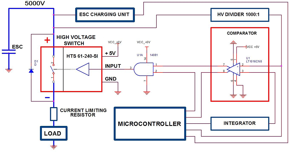
Figure 3. An example of a circuit for protecting a switching module from short-circuit currents using a system method.
The construction principle of this protection method resembles the structure used when employing a single transistor switch or parallel connection of transistor keys. In cases where high installation voltages (exceeding 1000 Volts) are involved, a powerful, low-resistance, non-inductive current-limiting resistor called the "CURRENT LIMITING RESISTOR" is incorporated into the circuit. This resistor serves to attenuate over currents during short circuit conditions.
Referring to the schematic solution shown in Figure 2, when there is a significant and excessively rapid discharge of the energy storage capacitor (ESC), which is detected by the comparator, the subsequent pulses from the microcontroller to the control input of the switching module are halted. To control the supply of control pulses to this input from the microcontroller, the logical element "AND" (U1A) is utilized. It enables or disables the delivery of control pulses to the control input of the module.