Introduction
Nanomaterial-based devices, characterized by their high surface-to-volume ratio, are highly sensitive to external factors, such as moisture and atmospheric contaminants1–4. To accurately assess their intrinsic electrical and optoelectronic properties, it is essential to conduct measurements under controlled environmental conditions, which often require high-vacuum systems. Although commercially available vacuum probe stations provide robust solutions for these measurements, they are prohibitively expensive for many research groups. Furthermore, their size and complexity often render them incompatible with glovebox environments, which are essential for the study of air-sensitive materials.
Recent advances in nanotechnology have spurred growing interest in the fabrication and characterization of devices entirely within controlled environments, such as gloveboxes, to prevent the degradation of air-sensitive materials during processing5–7. The ability to transfer the as-fabricated devices directly from a glovebox to a vacuum chamber without exposing them to ambient air offers a powerful advantage for maintaining material stability and ensuring reliable measurements. This requirement has driven the development of compact and customizable vacuum chamber systems.
Several efforts have been made to address this challenge. For instance, an inexpensive, thermally stable vacuum chamber utilizing Peltier devices has enabled high-precision electrical transport measurements, achieving millikelvin-level temperature control8. Similarly, a high-vacuum system specifically designed for testing 2D optoelectronic devices has demonstrated versatility with temperature modulation and broad-wavelength compatibility9. Advances in miniaturized systems have included designs with integrated on-chip vacuum chambers and graphene-based sealing for enhanced performance10. These studies emphasize the potential of compact and affordable solutions, but they fail to address the unique requirements of glovebox integration for air-sensitive nanodevices. Recently, a very compact suitcase filled with inert gas was reported11, it lacked electrical contacts for the in situ probing of air-sensitive devices.
Herein, we present a miniature vacuum chamber system designed to address this gap. Our system is sufficiently compact to fit within a glovebox, enabling the preparation and sealing of air-sensitive devices in an inert atmosphere before being transferred to vacuum conditions. It features a custom-built test board for three-terminal electrical-transport measurements tailored for field-effect transistors. Unlike existing solutions, our system is constructed primarily from commercially available contact-flange (CF) components, requires minimal modifications, and has a total cost of approximately €250. This design not only reduces the economic barrier for research groups, but also offers flexibility for testing a variety of nanodevices under controlled environments. The functionality of the system was demonstrated by characterizing a black phosphorus field-effect transistor fabricated and sealed under anaerobic conditions, ensuring no exposure to ambient air during the process.
Methods
Figure 1 shows a schematic of the different chamber components. The inset shows a picture of the vacuum chamber system with and without the windows. The total system length is approximately 30 cm, which makes it fit in the sample load lock of our anaerobic chamber7. The baseplate of the chamber was custom-modified in the mechanical workshop to include a homebuilt electrical feedthrough with four connections (suitable for the characterization of field-effect devices) and a port for vacuum pumping, which included a compact vacuum valve.
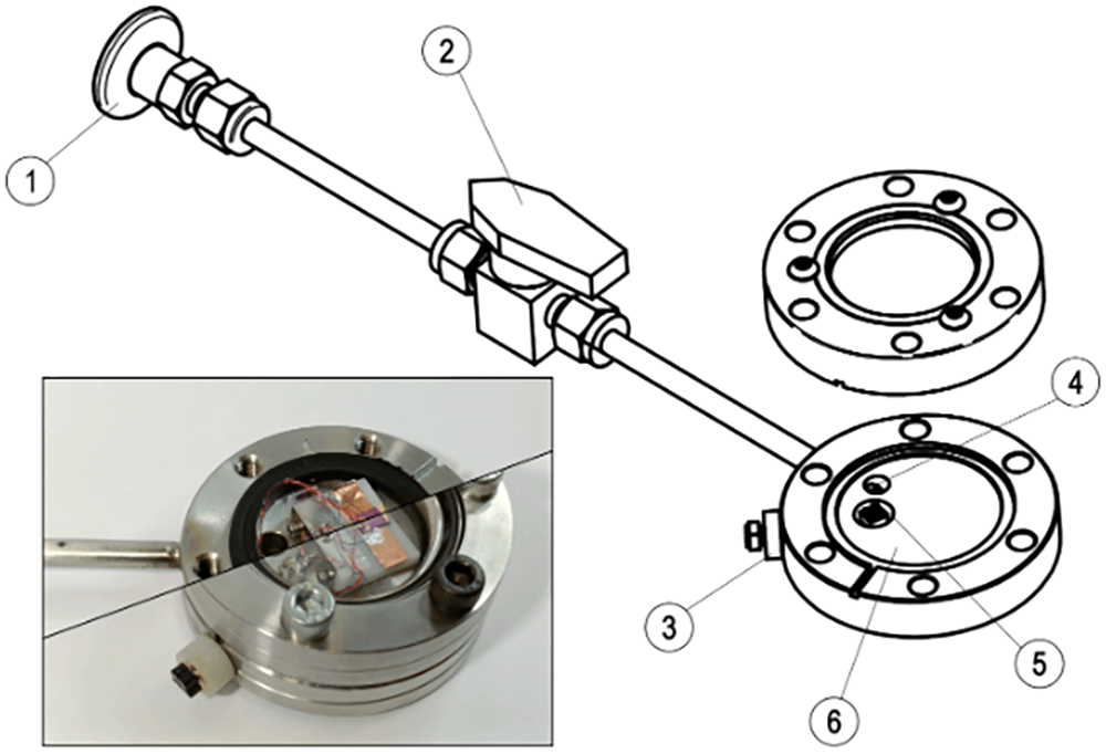
Figure 1. Description of the miniature vacuum chamber system.
Diagram of the miniature vacuum chamber system highlighting the different parts: (1) KF25 flange to connect to the vacuum pump, (2) Swagelok compact vacuum valve, (3) homebuilt electrical feedthrough, (4) vacuum port, (5) cabling port and (6) vacuum base plate to place the device test boards. (inset) Composite optical image of the vacuum chamber without (left) and with (right) the optical window on.
To fabricate the feedthrough, we started with a blank CF vacuum flange and drilled two aligned holes (one at the edge and one on the inner surface) so they met to form a continuous channel between the outside and inside of the chamber. Thin enamel-coated copper wires (magnetic wires) were threaded through this channel to create electrical paths. On the exterior (air side), the wires were soldered to a small PCB board fitted with pin sockets for convenient connection to the external instrumentation. The holes and wires were sealed using two-component epoxy resin (Nural 26) to maintain vacuum integrity. On the vacuum side, the wires were soldered to pin the sockets, allowing quick and tool-free connection/disconnection of the sample test board inside the chamber.
Figure 2a shows an optical image of the assembled test board mounted inside the vacuum chamber. The test board consisted of a machined polyoxymethylene (POM) base and an L-shaped stainless-steel top clamp (fabricated from a 0.5 mm thick 304 stainless steel sheet) held together with M1.6 screws. The compact footprint (20 mm × 24 mm, height ~10 mm) allows it to fit precisely into the recess machined into a vacuum flange. A copper strip was adhered to the base to enable contact with the back gate of the device via silver paint. The inset shows a schematic representation of the test board, highlighting the positioning of the cantilevered flexible contacts, springs, and screw mechanism.
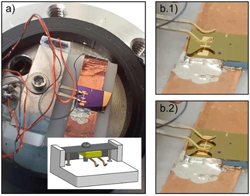
Figure 2. Test board to make electrical connections to electronic devices inside the miniature chamber.
(a) Optical image of the homebuilt test board with flexible cantilevered contacts to make electrical connections to devices. The test board base is supplemented with a copper tape to make electrical connection to the back-gate of the samples for field effect measurements. (inset) 3D sketch of the test board. (b.1) and (b.2) Optical images of the flexible cantilevered contacts when lifted (b.1) and landed (b.2) onto the electrodes. The height of the flexible cantilevers can be controlled with the screw shown in (a).
Mounted on the L-shaped clamp is a small 2 mm × 4 mm plate trimmed from a standard PCB, to which two phosphor bronze, gold-coated cantilevered flexible contacts are soldered with a separation of 2.5 mm. These cantilevered contacts provided a gentle and tunable electrical connection with the device pads. The rounded ends were designed to avoid scratching the pads during contact. The cantilevered contacts and associated coil springs, which allow vertical flexibility, were repurposed using a commercial SD card connector. An electrical connection to the test board was made via pin headers, which were also mounted on the PCB.
Figure 2(b.1) and (b.2) show close-up optical images of the flexible cantilevered contacts at the lifted (non-contact) and lowered (contact) positions, respectively. The vertical displacement of the cantilevered contacts was controlled via a screw mechanism, allowing reliable and repeatable engagement with the device electrodes without requiring fine motor precision, which is particularly advantageous for handling inside a glovebox.
We designed our test board to be compatible with electrical pads separated by 2.54 mm (a standard electrode distance for devices fabricated by evaporation using shadow masks manufactured by Ossila); however, it could have been fabricated to be compatible with other electrode pad pitch distances. It also allows for optical characterization, owing to the length of the cantilevered flexible contacts that make the sample fully accessible from the top viewport. The electrical connection to the back gate can be easily achieved through copper tape adhered to the base of the test board. Silver paint was used to connect the doped silicon substrate that was used as the back gate. This test board design facilitates electrical connection to devices, even when wearing thick gloves while operating inside a glovebox chamber. Once the flexible cantilevered contacts are lifted, the device is placed under the cantilevers, which are aligned with the pads of the chip below. The sample was then adhered to copper tape with silver paint to make a connection to the back-gate and to fix the sample and avoid movement while lowering the flexible pins with the screw.
Materials and methods
2D material exfoliation and transfer. BP flakes were mechanically exfoliated from bulk crystals (Smart Elements) using Nitto tape (Nitto SPV 224) onto a PDMS substrate (Gel-Film WF 4 × 6.0 mil by Gel-Pack). After flake selection and identification with an optical microscope in the transmission mode, the flakes were directly transferred from the PDMS to the final substrate between the prepatterned electrode pairs.
Electrode preparation. Source–drain electrodes were fabricated by shadow mask evaporation (5 nm Ti/45 nm Au) onto a SiO2 (285 nm)/Si (p++) substrate. The Ossila and E321 shadow masks were used in this study.
Electrical device characterization. In the electrical characterization of the device inside the miniature vacuum chamber, source–drain probing was achieved with a source-meter unit (Keithley 2450), while two programmable benchtop DC power supplies (Tenma 72–2715, connected in series) were used to apply gate voltages. Before acquiring the transport characteristics, the device was annealed on a hot plate (heating the miniature vacuum chamber) at 120 °C for 2 h.
Results
To illustrate the potential of this small vacuum chamber, we fabricated a field-effect transistor with black phosphorus inside an anaerobic chamber and mounted the as-fabricated device inside the miniature vacuum chamber to completely avoid exposing the device to air. After device fabrication and loading into the miniature vacuum chamber, the chamber was sealed in an anaerobic atmosphere. The vacuum chamber was then placed outside the anaerobic chamber, and the chamber was pumped down to ~7 × 10⁻⁶ mbar (Figure 3). We then characterized the field-effect characteristics of the black phosphorus transistor.
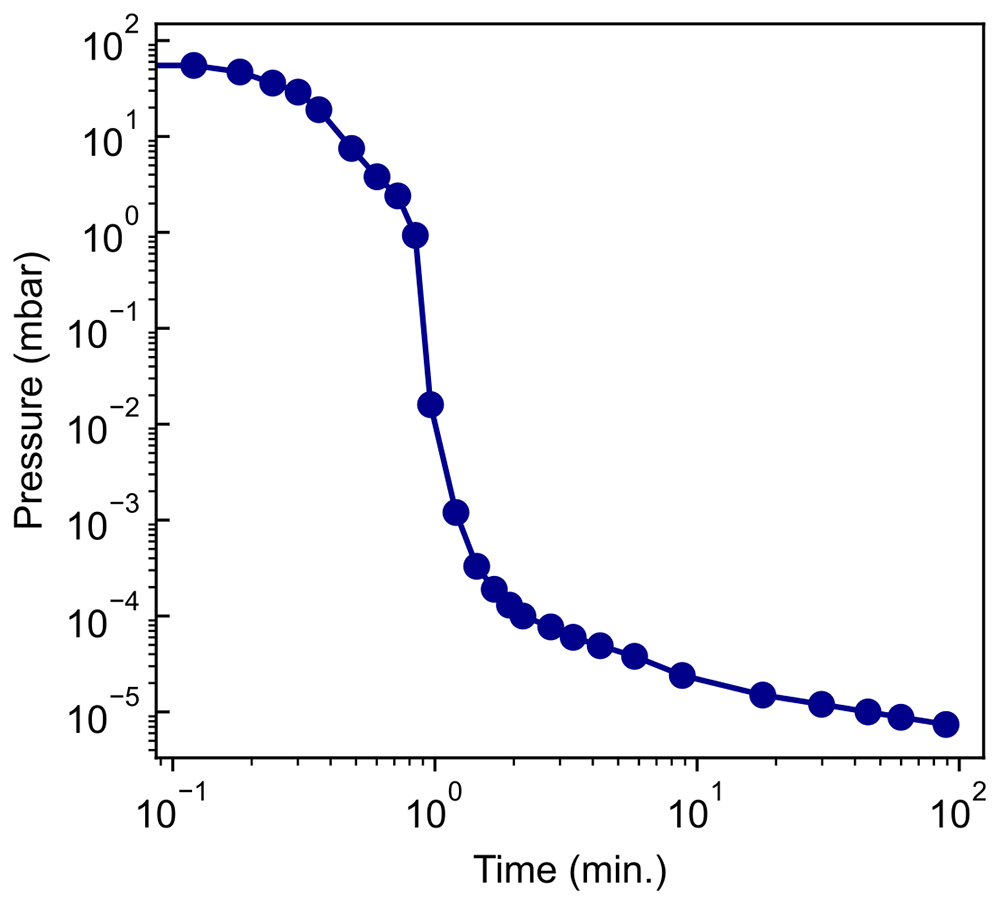
Figure 3. Fast pump-down of miniature vacuum chamber.
Logging of the pressure in the vacuum chamber over 1.5 hours. Pressures below 1 × 10⁻⁵ mbar are achieved within 30 minutes.
Figure 4a shows the gate-dependent transport characteristics of the black phosphorus field effect FET immediately after device fabrication. As black phosphorus is a p-type semiconductor, the channel conductance decreases as the gate voltage is swept from negative to positive values. The inset depicts the transfer curve for the device, where saturation of the source-drain current is not observed. After 15 d of storage in our custom miniature vacuum chamber (without further pumping), we repeated the electrical characterization of the device, as shown in Figure 4b. A moderate decrease (~50%) in device conductance was observed, both in the high- and low-conductance states, along with a 30 V shift in the transfer curve. This shift can be attributed to p-type doping induced by the adsorption of atmospheric species, such as oxygen, on the surface of the flake12,13. The observed degradation was likely due to the presence of residual gases inside the chamber, originating from the gradual outgassing of the internal surfaces. Because the materials and cleaning protocols of the chamber components were not fully optimized for ultrahigh vacuum performance, outgassing remains a plausible source of contamination over long storage times. This effect can be mitigated by implementing continuous pumping or by further optimizing the materials and preparation procedures to reduce the outgassing rates.
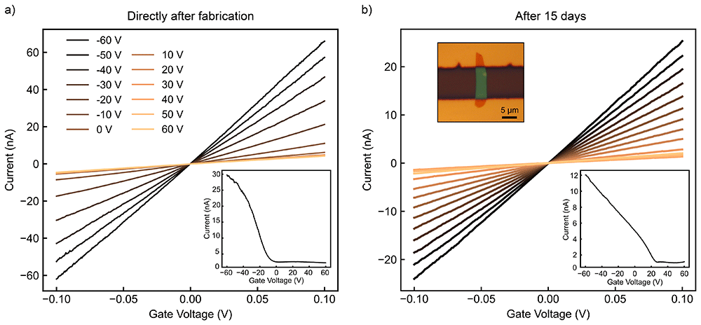
Figure 4. Example of electrical transport measurement in a black phosphorus device inside the miniature chamber.
(a) Gate dependent source-drain current vs. bias voltage characteristics in a black phosphorus device fabricated inside an anaerobic chamber and directly loaded inside the miniature vacuum system inside the chamber. (Inset) Source-drain current vs. gate voltage curve under 50mV of bias voltage. (b) Same electrical transport as shown in (a) after 15 days in vacuum inside the miniature vacuum system. (Top inset) Optical image of two-terminal field-effect transistor based on non-encapsulated, few-layer black phosphorus.
Notably, after 15 d, the ON/OFF ratio (ION/IOFF) of the device remained nearly unchanged, only decreasing by 10%. These findings contrast with the well-documented degradation of non-encapsulated black phosphorus thin flakes, whose conductivity dramatically worsens in timescales of 1–2 days14–16. Overall, the transport characteristics of the black phosphorus transistor illustrate the environmental stability of air-sensitive materials in the vacuum chamber.
Conclusions
The presented vacuum chamber system with electrical connections is an inexpensive and easy-to-implement solution for characterizing nanodevices under high-vacuum conditions. The compatibility of the system with glovebox environments provides an added advantage for studying air-sensitive materials, such as organic perovskites17,18 or high-temperature superconductors19–21. Our homebuilt sample test board makes it convenient to perform three-terminal electrical transport measurements and allows the study of the optoelectronic properties of field-effect transistors under focused illumination22. The performance of the system was demonstrated by characterizing a field-effect black phosphorus device prepared inside an anaerobic chamber and loaded into a vacuum chamber.
Data availability statement
Underlying data
Zenodo: Dataset for manuscript: Miniature vacuum chamber for electrical characterization of air-sensitive nanodevices, https://doi.org/10.5281/zenodo.1577680223
This project contains the following underlying data:
- Gate-dependent IV characteristics for black phosphorus field effect transistor
- Transfer curves for black phosphorus field effect transistor
- Pressure logging from miniature vacuum chamber pump-down
Data are available under the terms of the Creative Commons Attribution 4.0 International license (CC-BY 4.0).
Extended data
Zenodo: Dataset for manuscript: Miniature vacuum chamber for electrical characterization of air-sensitive nanodevices, https://doi.org/10.5281/zenodo.1577680223
This project contains the following underlying data:
- Details of the miniature vacuum chamber (item list & technical drawings)
- Images of use of the miniature vacuum chamber in the anaerobic gloveless chamber
- Additional pressure-logging of the pump-down of the miniature vacuum chamber
Data are available under the terms of the Creative Commons Attribution 4.0 International license (CC-BY 4.0).
Acknowledgments
Text edition with AI language model:
ChatGPT (GPT-4o, OpenAI’s large-scale language-generation model) was used to improve the English grammar and writing style of this manuscript. The authors have reviewed, edited, and revised the ChatGPT-generated texts to their own liking and took ultimate responsibility for the content of this publication.
Faculty Opinions recommendedReferences
- 1.
Wang G, Pandey R, Karna SP:
Physics and chemistry of oxidation of two‐dimensional nanomaterials by molecular oxygen.
WIREs Comput Mol Sci.
2017; 7(1): e1280. Publisher Full Text
- 2.
Yang S, Jiang C, Wei S:
Gas sensing in 2D materials.
Appl Phys Rev.
2017; 4(2): 021304. Publisher Full Text
- 3.
Zhao Q, Wang W, Carrascoso-Plana F, et al.:
The role of traps in the photocurrent generation mechanism in thin InSe photodetectors.
Mater Horiz.
2020; 7(1): 252–262. Publisher Full Text
- 4.
Li J, Peng S, Jin Z, et al.:
The effect of a vacuum environment on the electrical properties of a MoS2 back-gate field effect transistor.
Crystals.
2023; 13(10): 1501. Publisher Full Text
- 5.
Gray MJ, Kumar N, O'Connor R, et al.:
A cleanroom in a glovebox.
Rev Sci Instrum.
2020; 91(7): 073909. PubMed Abstract
| Publisher Full Text
- 6.
Wang W, Clark N, Hamer M, et al.:
Clean assembly of van der Waals heterostructures using silicon nitride membranes.
Nat Electron.
2023; 6: 981–990. Publisher Full Text
- 7.
Gant P, Carrascoso F, Zhao Q, et al.:
A system for the deterministic transfer of 2D materials under inert environmental conditions.
2D Mater.
2020; 7(2): 025034. Publisher Full Text
- 8.
Poole SF, Amin OJ, Solomon A, et al.:
Thermally stable Peltier controlled vacuum chamber for electrical transport measurements.
Rev Sci Instrum.
2024; 95(3): 035108. PubMed Abstract
| Publisher Full Text
- 9.
Zhao Q, Carrascoso F, Gant P, et al.:
A system to test 2D optoelectronic devices in high vacuum.
J Phys Mater.
2020; 3(3): 036001. Publisher Full Text
- 10.
Yu P, Zhan F, Rao W, et al.:
An on-chip microscale vacuum chamber with high sealing performance using graphene as lateral feedthrough.
Micromachines (Basel).
2022; 14(1): 84. PubMed Abstract
| Publisher Full Text
| Free Full Text
- 11.
Tirion S, Cheng Z, Pen C, et al.:
A technical note on a compact inert-gas suitcase for optical measurements of air-sensitive 2D materials. Publisher Full Text
- 12.
Li XB, Guo P, Cao TF, et al.:
Structures, stabilities, and electronic properties of defects in monolayer Black Phosphorus.
Sci Rep.
2015; 5: 10848. PubMed Abstract
| Publisher Full Text
| Free Full Text
- 13.
Lee BC, Kim CM, Jang HK, et al.:
Degradation pattern of Black Phosphorus multilayer field−effect transistors in ambient conditions: strategy for contact resistance engineering in BP transistors.
Appl Surf Sci.
2017; 419: 637–641. Publisher Full Text
- 14.
Island JO, Steele GA, van der Zant HSJ, et al.:
Environmental instability of few-layer Black Phosphorus.
2D Mater.
2015; 2(1): 011002. Publisher Full Text
- 15.
Wood JD, Wells SA, Jariwala D, et al.:
Effective passivation of exfoliated Black Phosphorus transistors against ambient degradation.
Nano Lett.
2014; 14(12): 6964–6970. PubMed Abstract
| Publisher Full Text
- 16.
Favron A, Gaufrès E, Fossard F, et al.:
Photooxidation and quantum confinement effects in exfoliated Black Phosphorus.
Nat Mater.
2015; 14(8): 826–832. PubMed Abstract
| Publisher Full Text
- 17.
Kojima A, Teshima K, Shirai Y, et al.:
Organometal halide perovskites as visible-light sensitizers for photovoltaic cells.
J Am Chem Soc.
2009; 131(17): 6050–6051. PubMed Abstract
| Publisher Full Text
- 18.
Schmidt-Mende L, Dyakonov V, Olthof S, et al.:
Roadmap on organic-inorganic hybrid perovskite semiconductors and devices.
APL Mater.
2021; 9(10): 109202. Publisher Full Text
- 19.
Charaev I, Bandurin DA, Bollinger AT, et al.:
Single-photon detection using high-temperature superconductors.
Nat Nanotechnol.
2023; 18(4): 343–349. PubMed Abstract
| Publisher Full Text
- 20.
Merino RL, Seifert P, Retama JD, et al.:
Two-dimensional cuprate nanodetector with single telecom photon sensitivity at T = 20 K.
2D Mater.
2023; 10(2): 021001. Publisher Full Text
- 21.
Ghosh S, Jangade DA, Deshmukh MM:
Nanowire bolometer using a 2D high-temperature superconductor.
Nanotechnology.
2023; 34(1): 015304. PubMed Abstract
| Publisher Full Text
- 22.
Pucher T, Bastante P, Xie Y, et al.:
Short-wave infrared photocurrent spectroscopy to probe narrow-gap 2D materials.
J Phys Appl Phys.
2025; 58(18): 185102. Publisher Full Text
- 23.
Luque Merino R, Riquelme JJ, Castellanos-Gomez A:
Dataset for manuscript: miniature vacuum chamber for electrical characterization of air-sensitive nanodevices.
Zenodo.
2025; 10.5281.